PCB Circuit Diagram APK for Android Download
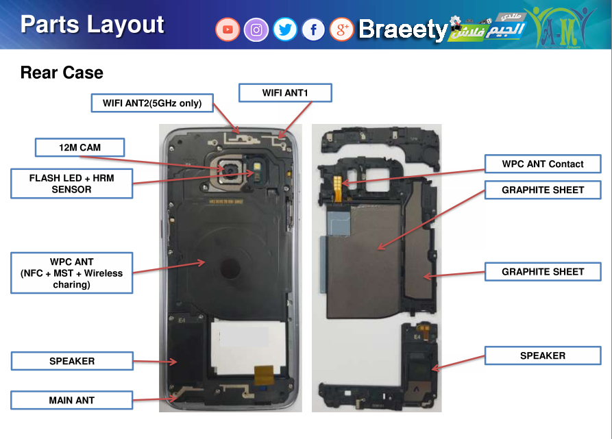
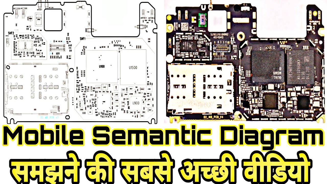
Mobile Phone PCB Layout Diagram How to Identify Parts and Components on the PCB (Motherboard) of a Mobile Cell Phone / Smartphone Network Section: The section below antenna point and above power section is called network section. 1. Antenna Point The point where antenna is connected is called antenna point.

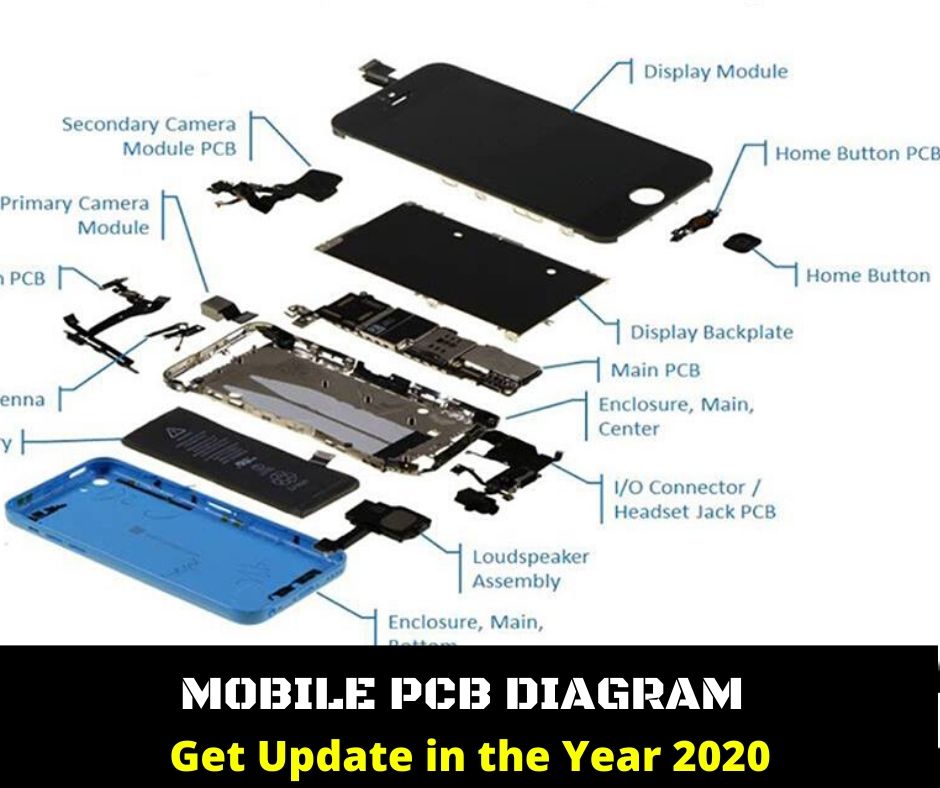
Mobile Phone PCB Diagram With Parts
Mobile circuit diagrams play a crucial role in the process of mobile repair. These diagrams provide a detailed visual representation of the internal circuitry and connections within a mobile phone.

Mobile Circuit Diagram Website
Figure 1-2: Cell-phone block diagram. (Speech, video, data) In Out D/A and A/D Converters and Filters Baseband devices that do not require an external power source in order to operate as passive devices; these include resistors, capacitors, and inductors.
Pcb Board Diagram All Mobile phone circuit board diagram Mobile Phone PCB Diagram with Parts
mobile circuit diagram book free download pdf is useful to the knowledge of Mobile Phone Troubleshooting

14 IPHONE 8 SCHEMATIC DIAGRAM AND PCB LAYOUT IphoneDiagram
Mobile Phone PCB Diagram with Parts Sections and Parts Inside a Mobile Cell Phone Mobile Phone Parts Identification | How to Identify Parts & Components on PCB of Mobile Phone Parts of a Mobile Cell Phone and Their Function (Big Parts) Small Parts / Electronic Components of Mobile Phone and Their Function Circuit Symbols of Electronic Components

All Mobile Circuit Diagram Software
Mobile PCB Diagram Free Download helps you identify mobile phone circuit board original parts and components.
Mobile Phone PCB Diagram With Part Mobile Repairing Online
Combinett: The Combinett Pro Schematics tool has PDF schematics to help mobile phone technicians. it has a special bitmap dual view and Ways Solutions to repair mobile phone hardware problems. Refox: Refox Schematic is a bitmap software program designed to help technicians with cell phone repair. It provides a comprehensive set of tools for.

[DIAGRAM] Nokia Mobile Pcb Diagram Guide
A Mobile Phone Block Diagram helps us to understand location of different parts of a mobile phone and the circuit. Use these Mobile Phone PCB Block Diagram T.

Free Download All Schematic PDF and Mobile PCB Diagram Smartphone repair, Phone solutions
All Mobile Circuit Diagram Software offers users the ability to design, simulate, repair, troubleshoot, and create custom circuit diagrams on their mobile devices. All Mobile Circuit Diagram Software puts powerful circuit design features in the palm of your hand. Engineers and hobbyists alike can quickly create accurate diagrams that can be.

Mobile Phone Diagram Pdf Techno Boz
UFSroom Schematic Diagram Tool v2.0.4 is a small free simple application for Windows computers that offers every mobile phone enthusiast, and professional or users to identify the most difficult fault paths and fix them. You can now use the tool-free version for three days.
How to download mobile PCB schematic diagram/service manual ? hindi YouTube
Laminate multilayer PCB fabrication technology is a type of multilayer PCB fabrication technology that is currently being widely applied. During the application of laminate multilayer PCB fabrication technology, substractive process is applied to manufacture circuit layer.
.jpg)
Mobile Phone PCB Diagram ESFY
DZKJ Schematics & PCB Layout - DZKJ PhoneRepair Tools. Professional Mobile Phone Schematic & PCB Layout. Update Help; A professional mobile phone repair information query tool, making repairs so easy! DZKJ Schematics Download New 1.0.0.51. 20M installation package, Download and register for 7-day free trial, You can try it first.

nokia 1110 layout diagram of pcb
A mobile schematic diagram is a type of graphic representation used to capture the electrical circuit of a mobile device. The diagrams are often composed of symbols connected by lines that depict the flow of electricity. When using mobile schematic software, these diagrams can be quickly generated and customized for whatever specific project or.
[35+] Vivo Y15 Schematic Diagram Custom Work Shirt
Save Palestine and Gaza from Israeli Terrorism Added Oppo A15 (CPH2185) Speaker & MIC & Earpiece Ways--- Added Samsung Galaxy A73 5G SM-A736B Charging NTC Thermistors Solution--- Added Samsung Galaxy A53 5G SM-A536B Charging Paused:Battery Temperature Too Low/High Problem Solution--- Added Samsung Galaxy A05 SM-A055F/A055M Block Diagram--- Added Realme C25Y (RMX3268) Charging&USB&Battery Ways.

(a) Circuit block diagram and (b) photographs of PCBA and PCBB for... Download Scientific
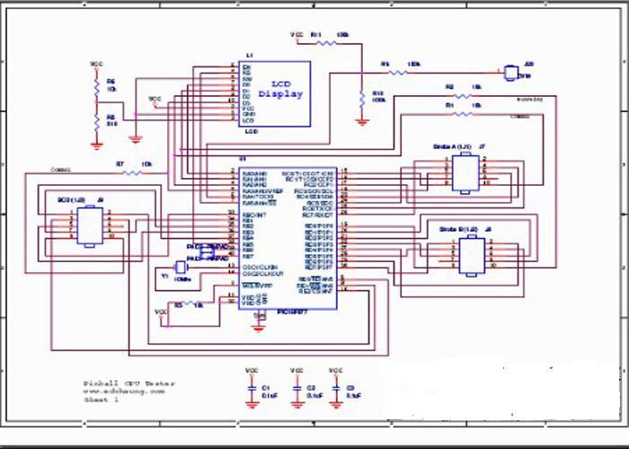
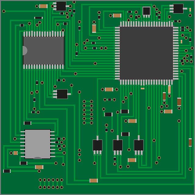
A mobile phone PCB diagram, also known as a printed circuit board diagram, is a graphical representation of the components and connections on the printed circuit board of a mobile phone. The PCB diagram provides a detailed and organized view of how the various electronic components are laid out and interconnected on the board.
[DIAGRAM] Intex Mobile Pcb Diagram
The RF section of a mobile PCB must be suitably separated and isolated from the power supply sections and from the digital or analog low power sections. Sensitive analog signals should also be kept as far away as possible from high-speed digital signals and from RF signals.